Three pitfalls in I2C
I recently implemented an I2C slave, and came across a few interesting corner cases in the specification.
I2C basics
I2C is a multi-master, low-speed, bidirectional bus specified in NXP UM10204. There are only two signals: SCL (the clock) and SDA (the data). Each of the signals is open-drain, with resistors pulling the signals high. This property is used throughout the protocol. For example, by defining an acknowledgement (ack) as holding SDA low, there is an implicit negative acknowledgement (nack) when no device responds to a transaction.
The general format of transactions is
-
a start condition
-
a 7-bit address
-
a read/write bit
-
an acknowledgement
-
any number of number of data bytes, each followed by an acknowledgement
-
a stop condition
For example, in the following diagram shows a single-byte read:
SDA is valid on the rising edge of SCL, and SDA changes on the falling edge of SCL. To signal the start and end of the transaction, SDA transitions with SCL high. This framing violation makes it easy to re-synchronize the master/slave state machines.
An important aspect of I2C that is not visible in the above diagram is who is sending data. Because the signals are open-drain, both the master and slave can drive the bus at the same time. The following diagram shows what the internal drivers of SDA in the above transaction might look like:
At the beginning of the transaction the master sends data on the bus, while the slave leaves its SDA high. Then the slave acknowledges the request and sends a byte of data. Since this is the last byte the master wants to read, the master doesn’t acknowledge the data and sends a stop condition.
Quick reads
One of the shortest types of I2C transactions is the quick read/write (so named by SMBus). These transfer one bit of data in the read/write bit following the address. Once the master receives an ack, it sends the stop condition to end the transaction. In addition to transfering a bit of data, these transactions can also be used as a heuristic way of detecting available slaves (such as with i2cdetect). The following diagram shows a successful quick read:
From the slave’s point of view, a quick read looks just like a regular read transaction. This can prevent the master from sending the stop condition if the first bit of the byte is a 0, since the slave will hold SDA low. If the read byte is all 0s, the slave won’t release SDA until the ack bit:
When designing a slave, this can be avoided by ensuring that the first bit of any read transaction is 1. If the slave has a “command” or sub-address register which needs to be written as the first byte of a transaction, the default data before the command register is written can be all 1s for the same effect.
From the master’s perspective, all that is needed is to continue reading out the byte until there is a high bit. This is guaranteed to happen when the slave waits for an ack.
SDA hold time ambiguity
While using coding violations for framing is a common technique, it creates a conflict on the falling edge of SCL. If a slave sees SDA fall before SCL, it can detect a spurious start/stop condition.
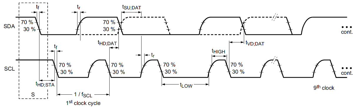
SMBus versions before 3.0 specified a 300 ns minimum hold time (tHD;DAT). This ensures that other devices on the bus see SCL transition before SDA.
I2C, on the other hand, has a minimum hold time of 0 seconds. Versions 6 and earlier of UM10204 suggested the following solution:
A device must internally provide a hold time of at least 300 ns for the SDA signal (with respect to the VIH(min) of the SCL signal) to bridge the undefined region of the falling edge of SCL.
That is, if a device detects a start/stop condition it must wait 300 ns before doing anything. If SCL is still high, it was a real start/stop. Otherwise it was just a data transition. The 300 ns value in both I2C and SMBus is tf, or the maximum fall time. Waiting this long ensures that SCL has transitioned before we sample SDA.
To allow for greater compatibility between SMBus and I2C devices, SMBus versions 3.0 and later reduce tHD;DAT to 0 seconds. In a lengthy appendix, they suggest using the same strategy as I2C.
Despite this, version 7 of UM10204 seems to suggest that neither a 300 ns hold time nor an internal delay are necessary to resolve this issue. Looking closely at the timing diagram, tHD;DAT is defined as the time between when SCL falls to 30% VDD (logical 0), and when SDA rises above 30% VDD or falls below 70% VDD. Therefore, it suggests that devices
Ensure SCL drops below 0.3 VDD on falling edge before SDA crosses into the indeterminate range of 0.3 VDD to 0.7 VDD.
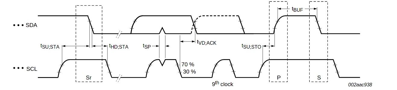
Regarding masters which don’t support clock stretching and don’t have inputs on SCL, UM10204 continues:
For controllers that cannot observe the SCL falling edge then independent measurement of the time for the SCL transition from static high (VDD) to 0.3 VDD should be used to insert a delay of the SDA transition with respect to SCL
effectively mandating a 300 ns hold time… which is what SMBus switched away from.
However, even masters supporting clock stretching should still use a delay for two reasons: First, it is difficult to detect when SCL falls below 30% VDD, since in typical implementations the entire region from 30–70% VDD is indeterminate. And second, devices with series protection resistors might not see the same value on SDA as the transmitter, since there will be a voltage difference across the resistor.
For maximum compatibility, devices should implement both an output hold time and an internal hold time when detecting start/stop conditions.
Implementation support
Unfortunately, despite much vacillation in SMBus and I2C, this issue does not seem to be known to some implementors. A quick survey of open-source implementations reveals fairly patchy handling:
-
Wikipedia’s bitbang implementation, doesn’t wait between
clear_SCLandset_SDAini2c_write_bit. That said, it doesn’t seem to support multi-master busses, so it may be assuming slaves with an internal hold time. -
Linux doesn’t wait between
sclloandsetsdaini2c_outb, but it doesn’t seem to support multi-master busses either. Some of the hardware-accelerated drivers seem to be aware of this issue, and support configurable hold times. This allows using the SMBus pre-3.0 solution, as long as all slaves also support it. -
Neither the master nor slaves in Alex Forencich’s I2C project seem to delay for a hold time or use an internal hold time.
-
Freecores’ master doesn’t add an internal hold time or use an internal hold time.
It’s often unclear whether commercial implementations correctly handle this ambiguity. For example, this AT24 EEPROM datasheet specifies a 0 second hold time, but doesn’t mention any internal hold time. Many vendors support configurable hold times, which shows they are aware of the issue. Occasionally, there are errata regarding it.
I suspect that for most hardware this ambiguity becomes an issue when the input threshold voltage is on the low end. This could cause a rising SDA to be detected before a falling SCL. This is exacerbated by high bus capacitance, but many busses have low (a few dozen pF) capacitance. As with many timing violations, mean time between failure can be quite long, and incorrect implementations may not be noticed.
Fast-mode Plus compatibility
The original (Standard-mode) I2C runs at 100 KHz, but UM10204 also includes a backwards-compatible “Fast-mode” which runs at 400 KHz. There are also “High-speed mode” and “Ultra Fast-mode” varients which are not backwards compatible. In 2007, NXP introduced a “Fast-mode Plus” which runs at 1 Mhz and was designed to be backwards-compatible. SMBus also incorporated this mode into version 3.0.
To determine what a Fast-mode Plus slave needs to do to be backwards compatible, let’s first examine Fast-mode backwards-compatibility. For a Fast-mode slave to be backwards compatible with Standard-mode, its input and output timings must be compatible with both Standard-mode and Fast-mode. Generally, output timings are the same as Fast-mode. Standard-mode only requires a longer setup time, which will be met as long as the slave doesn’t stretch the clock. Similarly, input timings are mostly the same as Fast-mode. One issue could be the internal hold time necessary for the SDA ambiguity detailed above. However, both Standard- and Fast-mode specify a 300 ns fall time (tf), which is less than Fast-mode’s 600 ns start condition setup time (tSU;STA). Therefore, the same 300 ns hold time can be used for both modes.
Unfortunately, Fast-mode Plus reduced tSU;STA to 260 ns in order to achieve a higher clock rate. This means that every Fast-mode Plus start condition is within the SDA hold time ambiguity in Fast- and Standard-mode. A slave which implements the 300 ns internal delay required by Fast- and Standard-mode will not be able to detect Fast-mode Plus start conditions with minimum-specified delay.
There are some ways to mitigate this at the system level:
-
All bust masters could be configured to run at 960 kHz, which (if tSU;STA is scaled as well) will provide enough of a delay to ensure start times will be detected correctly.
-
Components with higher slew rates could be selected to ensure tf remains below 260 ns. Alternatively, bus line capacitance could be reduced below the maximum.
As well as some ways to mitigate this at the device level:
-
A configuration bit (such as a register or a pin) could configure the device to be either Fast-mode or Fast-mode Plus compatible. This could even be automatically detected, although this would need to be done carefully since masters can switch speed at any time. For example, a master might run at one speed when accessing a certain device, and another speed when accessing a different device.
-
The input drivers could be engineered to have a lower VIH and a higher VIL, reducing the time of ambiguity (assuming monotonic transitions).
But, as-written, the Fast-mode Plus timings are incompatible with Fast- and Standard-mode. Pre-3.0 SMBus and post-v7 I2C are not affected because they do not require an internal hold time.